- 您现在的位置:买卖IC网 > Sheet目录341 > MAX6948BGWA+T (Maxim Integrated)IC LED DVR PWM GPIO 25WLP
�� �
�
�MAX6948B�
�High-Efficiency� PWM� LED� Driver� with� Boost�
�Converter� and� Five� Constant-Current� GPIO� Ports�
�Boost� Converter�
�Boost-Converter� Output� PWM�
�The� MAX6948B� boost� converter� has� 10-bit� PWM� opera-�
�tion� using� an� internal� 125kHz� clock.� This� yields� a� PWM�
�period� of� 1024/125k� =� 8.192ms.� PWM� operation� allows�
�the� user� to� adjust� the� LED� intensity� and� lower� the� average�
�current� by� enabling� and� disabling� the� boost� converter� at�
�a� selectable� rate.� This� rate� is� set� using� the� boost-con-�
�verter� output� PWM� registers� (Tables� 4,� 5).� The� duty� cycle�
�ranges� from� 0/1024� (no� intensity� or� off)� to� 1023/1024� (full�
�intensity).� Eight� of� the� 10� bits,� which� include� the� MSB,� are�
�in� a� single� register� (0x20)� to� allow� a� single� I� 2� C� write� to�
�set� the� majority� of� the� intensity� level� and� minimize� visible�
�flicker� during� intensity� changes.� The� LSB� register� (0x21)�
�allows� for� very� fine� adjustments� in� LED� intensity.�
�Boost-Converter� Status� Register�
�The� MAX6948B� checks� the� boost� converter� and� indi-�
�cates� its� status� in� the� boost-converter� status� register�
�(Table� 6).� Faults� indicated� in� this� register� include� ther-�
�mal� shutdown,� overvoltage,� and� current� limit.� The� boost�
�converter� goes� into� standby� mode� whenever� the� boost�
�standby� bit� (D0)� =� 1.�
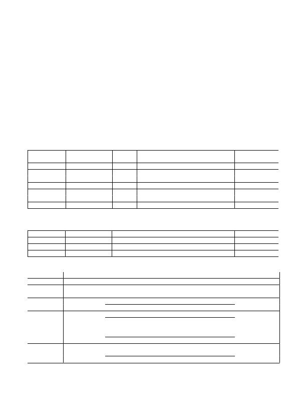
�Table� 4.� Boost-Converter� Output� PWM� (MSB)� Register� Format� (0x20)�
�REGISTER� BIT�
�D7�
�D6�
�D5�
�D4�
�D3�
�D2�
�D1�
�D0�
�DESCRIPTION�
�Bit� 9�
�Bit� 8�
�Bit� 7�
�Bit� 6�
�Bit� 5�
�Bit� 4�
�Bit� 3�
�Bit� 2�
�VALUE�
�—�
�—�
�—�
�—�
�—�
�—�
�—�
�—�
�FUNCTION�
�Boost-converter� output� PWM� bit� 9� (MSB)�
�Boost-converter� output� PWM� bit� 8�
�Boost-converter� output� PWM� bit� 7�
�Boost-converter� output� PWM� bit� 6�
�Boost-converter� output� PWM� bit� 5�
�Boost-converter� output� PWM� bit� 4�
�Boost-converter� output� PWM� bit� 3�
�Boost-converter� output� PWM� bit� 2�
�DEFAULT� VALUE�
�0�
�0�
�0�
�0�
�0�
�0�
�0�
�0�
�X� =� Don’t� care.�
�Table� 5.� Boost-Converter� Output� PWM� (LSB)� Register� Format� (0x21)�
�REGISTER� BIT�
�D7–D2�
�D1�
�D0�
�DESCRIPTION�
�Reserved�
�Bit� 1�
�Bit� 0�
�VALUE�
�000000�
�—�
�—�
�FUNCTION�
�—�
�Boost-converter� output� PWM� bit� 1�
�Boost-converter� output� PWM� bit� 0� (LSB)�
�DEFAULT� VALUE�
�000000�
�0�
�0�
�Table� 6.� Boost-Converter� Status� Register� Format� (0x22)�
�REGISTER� BIT�
�D7,� D6,� D5�
�D4�
�D3�
�DESCRIPTION�
�Reserved�
�Schottky� open�
�Current� limit�
�VALUE�
�000�
�0�
�1�
�0�
�1�
�FUNCTION�
�—�
�Schottky� diode� present�
�Schottky� diode� open�
�Normal� output� current�
�Converter� output� current� exceeded� the� current� limit�
�DEFAULT� VALUE�
�000�
�Read� only�
�Read� only�
�0�
�Normal� operation�
�D2�
�D1�
�D0�
�Thermal� shutdown�
�Overvoltage�
�Boost� standby�
�1�
�0�
�1�
�0�
�Device� temperature� has� exceeded� thermal�
�shutdown� threshold�
�Normal� operation�
�V� OUT� exceeded� overvoltage� limit�
�Boost� converter� operating� according� to� PWM�
�register� and� configuration� register�
�Read� only�
�Read� only�
�1�
�12�
�1�
�Boost� converter� in� standby� mode�
�Maxim� Integrated�
�发布紧急采购,3分钟左右您将得到回复。
相关PDF资料
MAX6964ATG+T
IC LED DRIVER LINEAR 24-TQFN
MAX6965ATE+T
IC LED DRIVER LINEAR 16-TQFN
MAX6967ATE+
IC LED DRIVER LINEAR 16-TQFN
MAX6968AAE+
IC LED DRIVER LINEAR 16-SSOP
MAX6970AUE+
IC LED DRIVER LINEAR 16-TSSOP
MAX6971AUG+T
IC LED DRIVER LINEAR 24-TSSOP
MAX6974ATL+
IC LED DRIVER LINEAR 40-TQFN
MAX6977AAE+
IC LED DRIVER LINEAR 16-SSOP
相关代理商/技术参数
MAX694C/D
功能描述:监控电路 RoHS:否 制造商:STMicroelectronics 监测电压数: 监测电压: 欠电压阈值: 过电压阈值: 输出类型:Active Low, Open Drain 人工复位:Resettable 监视器:No Watchdog 电池备用开关:No Backup 上电复位延迟(典型值):10 s 电源电压-最大:5.5 V 最大工作温度:+ 85 C 安装风格:SMD/SMT 封装 / 箱体:UDFN-6 封装:Reel
MAX694CPA
功能描述:监控电路 RoHS:否 制造商:STMicroelectronics 监测电压数: 监测电压: 欠电压阈值: 过电压阈值: 输出类型:Active Low, Open Drain 人工复位:Resettable 监视器:No Watchdog 电池备用开关:No Backup 上电复位延迟(典型值):10 s 电源电压-最大:5.5 V 最大工作温度:+ 85 C 安装风格:SMD/SMT 封装 / 箱体:UDFN-6 封装:Reel
MAX694CPA+
功能描述:监控电路 MPU Supervisor RoHS:否 制造商:STMicroelectronics 监测电压数: 监测电压: 欠电压阈值: 过电压阈值: 输出类型:Active Low, Open Drain 人工复位:Resettable 监视器:No Watchdog 电池备用开关:No Backup 上电复位延迟(典型值):10 s 电源电压-最大:5.5 V 最大工作温度:+ 85 C 安装风格:SMD/SMT 封装 / 箱体:UDFN-6 封装:Reel
MAX694EJA
功能描述:监控电路 RoHS:否 制造商:STMicroelectronics 监测电压数: 监测电压: 欠电压阈值: 过电压阈值: 输出类型:Active Low, Open Drain 人工复位:Resettable 监视器:No Watchdog 电池备用开关:No Backup 上电复位延迟(典型值):10 s 电源电压-最大:5.5 V 最大工作温度:+ 85 C 安装风格:SMD/SMT 封装 / 箱体:UDFN-6 封装:Reel
MAX694EPA
功能描述:监控电路 RoHS:否 制造商:STMicroelectronics 监测电压数: 监测电压: 欠电压阈值: 过电压阈值: 输出类型:Active Low, Open Drain 人工复位:Resettable 监视器:No Watchdog 电池备用开关:No Backup 上电复位延迟(典型值):10 s 电源电压-最大:5.5 V 最大工作温度:+ 85 C 安装风格:SMD/SMT 封装 / 箱体:UDFN-6 封装:Reel
MAX694EPA+
功能描述:监控电路 MPU Supervisor RoHS:否 制造商:STMicroelectronics 监测电压数: 监测电压: 欠电压阈值: 过电压阈值: 输出类型:Active Low, Open Drain 人工复位:Resettable 监视器:No Watchdog 电池备用开关:No Backup 上电复位延迟(典型值):10 s 电源电压-最大:5.5 V 最大工作温度:+ 85 C 安装风格:SMD/SMT 封装 / 箱体:UDFN-6 封装:Reel
MAX694MJA
功能描述:监控电路 RoHS:否 制造商:STMicroelectronics 监测电压数: 监测电压: 欠电压阈值: 过电压阈值: 输出类型:Active Low, Open Drain 人工复位:Resettable 监视器:No Watchdog 电池备用开关:No Backup 上电复位延迟(典型值):10 s 电源电压-最大:5.5 V 最大工作温度:+ 85 C 安装风格:SMD/SMT 封装 / 箱体:UDFN-6 封装:Reel
MAX694MJA/883B
功能描述:监控电路 MPU Supervisor RoHS:否 制造商:STMicroelectronics 监测电压数: 监测电压: 欠电压阈值: 过电压阈值: 输出类型:Active Low, Open Drain 人工复位:Resettable 监视器:No Watchdog 电池备用开关:No Backup 上电复位延迟(典型值):10 s 电源电压-最大:5.5 V 最大工作温度:+ 85 C 安装风格:SMD/SMT 封装 / 箱体:UDFN-6 封装:Reel